


Moldex3D模流分析之分析毛細底部填膠制程中不同材質流動接觸角的影響 
Flip-chip capillary underfilling process 操作流程 ─ 在填膠分析中,不同嵌件材料的的接觸角設定 步驟1:首先建立一個芯片封裝成型項目,并匯入毛細底部填膠模型。
2323 2 1
Moldex3D 中國 ??? 2年前
HFSS 3D Layout:輕松實現從系統級求解芯片設計 
本文原刊登于Ansys Blog:《Solving Chip Designs at the System Level via HFSS 3D Layout》 作者:Aaron Edwards | Ansys高級應用工程經理 編輯整理:趙陽 | Ansys中國技術支持工程師 使用Ansys HFSS 3D Layout只需34個小時,就能生成并求解上方這個復雜的
3485 1 1
CAE聯盟新聞 ??? 4年前
仿真案例 | 芯片近場掃描模擬仿真 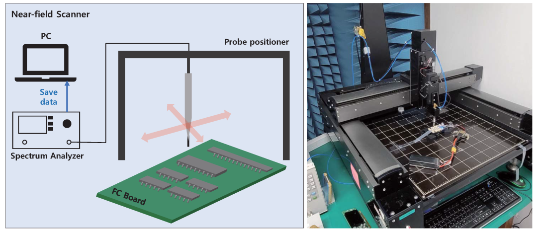
04近場結果 在Circuit仿真結束后,即可將時域的仿真結果Push至HFSS工程中; 選中前面繪制的sheet,Create Field Plot; 以下,通過仿真得到基板上該組差分走線傳輸PRBS信號時,在芯片上方附近產生的電場分布圖; 可以看到,由于在Circuit中的激勵是由BGA向Chip傳輸,因此在任意頻點下
4278 3
萬有引力LYQ ??? 2年前
2025大賽優秀作品 | 基于Ansys的XDFOI晶圓級封裝工藝的翹曲模擬與實驗驗證 
warpages in glass detached process Increasing the CTE of UF would reduce the WLP wafer warpage Decreasing the CTE and Young’s modulus of glass would significantly decrease the warpage in stage 2, flip
1343
Ansys中國 ??? 2月前
仿真案例 | 芯片近場掃描模擬仿真
04近場結果 在Circuit仿真結束后,即可將時域的仿真結果Push至HFSS工程中; 選中前面繪制的sheet,Create Field Plot; 以下,通過仿真得到基板上該組差分走線傳輸PRBS信號時,在芯片上方附近產生的電場分布圖; 可以看到,由于在Circuit中的激勵是由BGA向Chip傳輸,因此在任意頻點下
2729 5
仿真客 ??? 2年前
仿真案例 | 芯片近場掃描模擬仿真
04近場結果 在Circuit仿真結束后,即可將時域的仿真結果Push至HFSS工程中; 選中前面繪制的sheet,Create Field Plot; 以下,通過仿真得到基板上該組差分走線傳輸PRBS信號時,在芯片上方附近產生的電場分布圖; 可以看到,由于在Circuit中的激勵是由BGA向Chip傳輸,因此在任意頻點下
3689 2
萬有引力LYQ ??? 2年前
用對了版本電磁3D仿真速度可提升10倍 
關于Ansys CPS 解決方案 Ansys CPS(Chip+Package+System)多物理場仿真方案,包含了Redhawk/HFSS等業界黃金工具,基于CPM/CSM/CTM等獨有的芯片模型,通過協同仿真考察芯片與PKG/PCB之間的耦合影響,通過電、熱、結構之間的多物理場耦合仿真使得仿真精度更高,幫助設計者優化從芯片至系統的
2619 1
Ansys中國 ??? 4年前
是否需要對IC開展電磁仿真?Ansys有話說~ 
關于Ansys CPS 解決方案 Ansys CPS(Chip
2589
CAE聯盟新聞 ??? 4年前
CINNO Research | 2022年上半年全球半導體封測廠商營收排名Top10 
公司將持續保持Flip Chip及先進封測技術在邏輯芯片業務上的發展。No.5:通富微電(TFME)營業收入同比增長約33.4%,位居第五。通富微電封測營收大幅增長得益于各大基地同步實現突破,崇川工廠、南通通富、合肥通富及通富超威都各自完成了眾多新產品的導入和量產及關鍵客戶的突破,同時預計下半年將小規模量產客戶5nm產品。
2077
CINNO ??? 3年前
先進芯片、Interposer和封裝設計的電磁與電路RLCK提取和仿真 
Anand答復說: “RaptorH桌面對當前RaptorX和HFSS用戶而言并不陌生,3D設計幾何結構和電磁場可視化解決方案使用了現有的Ansys桌面界面。” Anand繼續說道: “S參數和電路網表模型都已提供。特別值得注意的是,該分析是在LVS之前開展的,而設計仍在進行中。” 我問道:“對于一般電磁分析,HFSS通常需要掌握大量的控制專業知識。
3028 1 1
Ansys中國 ??? 4年前
2.5D/3D芯片-封裝-系統協同仿真技術研究 
系統級芯片(system on chip, SoC)與系統級封裝 (system in package,SiP)都是實現更高性能,更低成本的方式[2],其中以三維立體封裝為代表的先進封裝技術將是后摩爾時代的核心驅動力之一,當前有多種3D堆疊技術,包括Bond wire, Flip chip及TSV等 [7] 。
6067 5 1
Ansys中國 ??? 4年前
30年間高頻電磁仿真創新歷程 
關于Ansys CPS 解決方案 Ansys CPS(Chip+Package
3390
Ansys中國 ??? 4年前
LED|Sharp/NEC推出新款直視LED顯示屏系列 
新FC系列采用的發光芯片使用了倒裝方式封裝(Flip-Chip Packaging),而將發光芯片直接鍵合在電路板上的方式也常叫做板上芯片(COB,Chip-on-board)技術,相對于傳統的LED芯片和鍵合技術,新方案具有更高的防碰撞、防靜電、防水漬和防灰塵等性能。這意味著它將具有更好的耐久性,而在零售和大眾運輸終端等人流量密度很高的空間,它將能讓顯示屏幕更加靠近人們的視線。
2017
CINNO ??? 3年前
Ansys在芯片/封裝結構熱力可靠性方案 
封裝結構的熱力可靠性方案 Influence of flip-chip attachment process on IC Moisture Diffusion\Moisture Stress Thermal Cycling\Thermal Stresses
2412
Cruise ??? 3年前
技術分享丨淺談SiP系列-工藝技術篇 
SiP主流的封裝結構形式 SiP主流的封裝形式有可為多芯片模塊(Multi-chipModule;MCM)的平面式2D封裝,2D封裝中有Stacked Die Module、Substrate Module、FcFBGA/LGA SiP、Hybrid(flip chip+wirebond)SiP-single sided、Hybrid SiP-double sided
3615 2 2
圖元TOPBRAIN ??? 3年前
Moldex3D模流分析之嵌入式晶圓級封裝制程(eWLP) 
晶圓級封裝非導電性黏著底部填膠 (Underfill)底部填膠技術 (Underfill) 是覆晶封裝成型 (Flip-Chip) 的制程之一。底部填膠區域夠薄以進行毛細應用,且沿著芯片的一側或兩側的周圍進行環氧塑料放置。表面張力與熱,是主要對底部填膠產生毛細作用的兩項物理因素。
2434 1
Moldex3D 中國 ??? 1年前
PCB | 興森科技在廣州設立FC-BGA工廠,計劃2025年稼動 
Chip Ball Grid Array)工廠。
1640
CINNO ??? 4年前
案例35-無鉛焊接凸點的彈塑性蠕變分析 
Creep behaviors of flip chip on board with 96.5Sn-3.5Ag and 100In lead-free solder joints. International Journal of Microcircuits and Electronic Packaging. 24: 11-18.
2694 8 5
龍飛宇 ??? 3年前
日本半導體封裝材料集體發力車載市場:住友電木/昭和電工/信越化學規劃信息匯總 
最初的DRAM采用的是BoC(Board on Chip)結構,隨著“倒裝芯片(Flip Chip)”趨勢的發展,MUF材料的需求不斷增長。如今,DRAM方向的MUF材料的占比最高。NAND方向顆粒狀材料需求也在增長。預計未來SiP和WLP(Wafer Level Package,晶圓級封裝)方向的需求會持續增長。
2639
CINNO ??? 3年前
從注塑成型到IC封裝,制程數字分身為何如此重要? 
encapsulation, Computers & Fluids 44 (2011) 187–201 [5].Nordson ASYMTEK: The NexJet System - Flip Chip Underfill:https://www.youtube.com/watch?
2573 3
ACMT協會 ??? 2年前
20條/頁 
跳至頁


技術鄰APP
工程師必備
工程師必備
- 項目客服
- 培訓客服
- 平臺客服
TOP
